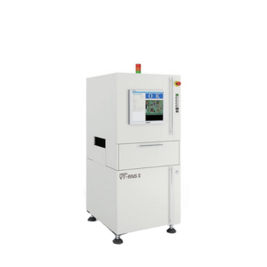
OMRON VT-RNS2 In-Line AOI Machine
Vintage:
PCB Direction: Left to Right
Condition: Refurbished, working
Running Hours:
Series Number:
Missing Parts: No
Warranty: 6 Months after instllation
Location: China
Lead time: 7 Days
SMT AOI/SMD AOI/SMT AOI Machine OMRON VT-RNS2
Fast production system startup and stable operation with no downtime.
Inspection system performance is the key.
The VT-RNS II delivers outstanding performance at every step of production. Easy-to-set initial inspection parameters are ready for immediate use to perform high accuracy inspections. Data collected from the inspection stations can be analyzed for root cause analysis of defects for ongoing process improvement.
Omron gives you the tools to increase productivity on your PCB assembly lines.
Quick Setup
Features EzTS for simple automated generation of inspection programs
The easy-to-use Ez-Image Teaching (Ez-IT) inspection program generation software is equipped as a standard feature, enabling anyone to quickly and easily create inspection programs tailored to the PCB. The software also validates the inspection programs so that they can be implemented on the production line without delay.
Faster
Improved image processing for faster post-reflow inspections
In addition to processing faster than that of conventional models, the VT-RNSII also features revamped imaging processes to achieve significantly faster outcomes.
This enables the system to cope with the most demanding production environments
Highly Accurate
Uses Omron’s 3-CCD and Color Highlight Technology
Omron pioneered the development of 3-CCD and Color Highlight Technology in PCB inspection systems to obtain correct measurements with high levels of inspection accuracy.
Expandable
Q-upNavi provides total support for process improvement, root cause defect analysis and countermeasure implementation
Q-upNavi is quality control software that analyzes inspection results and provides feedback to the production line. This software enables operators to implement corrective procedures that will prevent future defects from occurring regardless of their level of experience or expertise.
Hardware Configuration
| | M size | L size |
|---|
| P/Z/S |
|---|
Image signal
input unit | Camera | 3-CCD camera |
|---|
| Illumination | Ring-shaped LEDs (R, G, B) |
|---|
| Image resolution | 10, 15, 20 μm |
|---|
| Main unit | Feed method | Belt |
|---|
| Line height | 900 ±15 mm |
|---|
PCB carrier width
adjustment | Automatic |
|---|
| PCB fixing method | Outer frame |
|---|
| Power supply | AC 100/115 V /120 V/200 V/220 V/230 V/240 V ±10% (single phase) |
|---|
| Air | 0.4 to 0.6 Mpa |
|---|
| Ambient operating temperature | +10 to +35°C |
|---|
| Ambient operating humidity | 35 to 80% RH (with no condensation) |
|---|
| Weight | Approx. 500 kg | Approx. 650 kg |
|---|
| Dimensions | 700 (W) × 900 (D) × 1,600 (H) mm
(Excluding Patlite signal tower) | 920 (W) × 1,365 (D) × 1,600 (H) mm
(Excluding Patlite signal tower) |
|---|
Functional Specifications
| | M size |
|---|
| P | Z | S |
|---|
Inspectable
PCBs | Type | Post-printing | Post-placement
(before reflow) | Post-reflow |
|---|
| Dimensions | 50 (W) × 50 (D) to 333 (W) × 255 (D) mm |
|---|
| Thickness | 0.3 to 2.5 mm |
|---|
| Clearance | Above PCB: 20 mm (0.79 in) (standard), 40 mm (1.57 in) (optional)
Below PCB: 40 mm (1.57 in) |
|---|
| Inspection items | Presence of solder,
insufficient/excessive
solder, solder shifting,
grazing, bridging,
spreading, leaking | Presence of solder,
component shifting, polarity
error, missing components,
wrong components, solder
balls, skewing, bridging,
foreign objects | Presence of solder, wrong
components, missing
components, bridging, lifting,
component shifting, fillets,
wettability, lead bending,
adhesive, solder balls |
|---|
| Number of inspection points | 40,000 lands/PCB max. | 10,000 components/PCB max. |
|---|
| Data storage | Computer hard disk |
|---|
Component-specific
inspection data library | Component types, groups, variations |
|---|
| Inspection result output | PCB name, PCB ID, component name, type of fault, etc. |
|---|
| Communications | Ethernet, RS-232C |
|---|
| PCB feed mode | Through, turnback |
|---|
| Reference position | PCB feed direction: left or right (selected at shipment);
Longitudinal: Front or back (selected at shipment) |
|---|
| | L size |
|---|
P | Z | S |
|---|
Inspectable
PCBs | Type | Post-printing | Post-placement (before reflow) | Post-reflow |
|---|
Dimensions | 80 (W) × 50 (D) to 510 (W) ×460 (D) mm 80 (W) × 110 (D) to 510 (W) ×460 (D) mm (with PCB warpage correction unit) |
|---|
Thickness | 0.3 to 3.0 mm |
|---|
Clearance | Above PCB: 20 mm (0.79 in) (standard), 40 mm (1.57 in) (optional) Below PCB: 50 mm (1,97 in) |
|---|
Inspection items | Presence of solder, insufficient/excessive solder, solder shifting, grazing, bridging, spreading, leaking | Presence of solder, component shifting, polarity error, missing components, wrong components, solder balls, skewing, bridging, foreign objects | Presence of solder, wrong components, missing components, bridging, lifting, component shifting, fillets, wettability, lead bending, adhesive, solder balls |
|---|
Number of inspection points | 40,000 lands/PCB max. | 10,000 components/PCB max. |
|---|
Data storage | Computer hard disk |
|---|
Component-specific
inspection data library | Component types, groups, variations |
|---|
Inspection result output | PCB name, PCB ID, component name, type of fault, etc. |
|---|
Communications | Ethernet, RS-232C |
|---|
PCB feed mode | Through, turnback |
|---|
Reference position | PCB feed direction: left or right (selected at shipment); Longitudinal: Front or back (selected at shipment) |
|---|